Home
Quickstart Guide
Introduction RIO Academic RIO Application examples Your first RT app Your first FPGA app
Real-Time
Basic procedures System admin File system I/O monitor System controller architecture Timed loops Inter-process communication RT/Host communication RT/FPGA communication FPGA personalities Interrupts Datalogger (file I/O)
FPGA
Design flow Simulation Inter-process communication RT/host communication Derived clock domain IP blocks FPGA personality
Networking
Get connected Email Web services UDP TCP IP addresses
Site Map
Guides Code examples Procedures Tags LabVIEW block diagram elements Targets Communications All pages
Glossary How to use About
RIO Developer Essentials Guide for Academia

"FPGA" target

Develop an FPGA VI
FPGA guide

Develop your own FPGA-targeted VI to take advantage of the unique capabilities of the FPGA target such as high-speed I/O, precision I/O timing, parallel processing, and functionality not offered by the RT processor and Academic RIO Device Toolkit default personality; you can also augment the default personality with your needed capability.
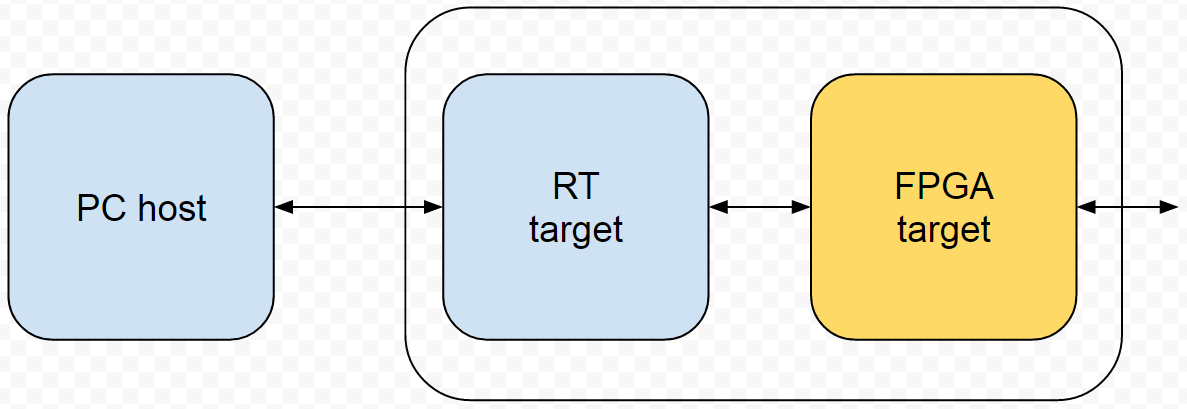
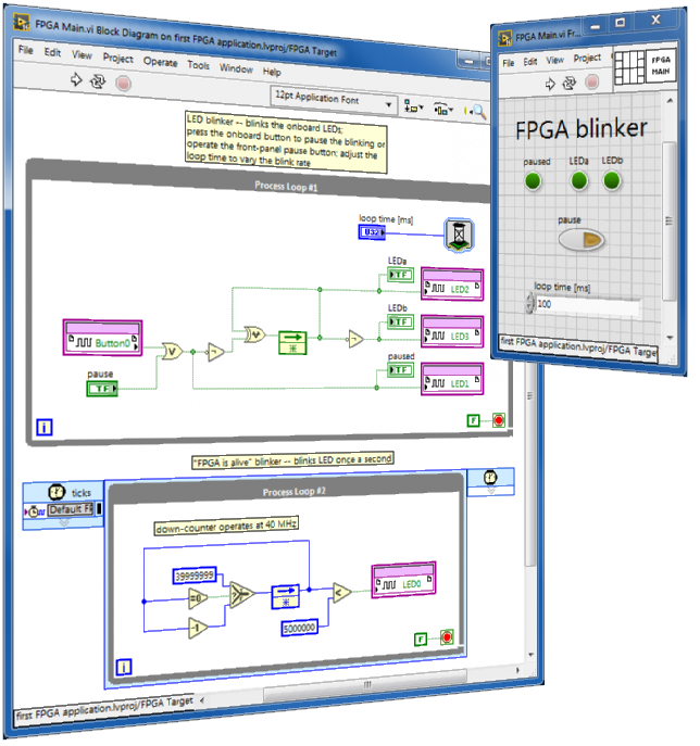
Follow along with this step-by-step tutorial to make a "hello, world!"-like application to experience the advantages of multiple linked VIs running simultaneously on the FPGA target, real-time (RT) target, and desktop computer: (1) "FPGA Main" VI blinks the onboard LEDs and reads the onboard button; these onboard devices physically connect to the FPGA I/O pins, (2) "FPGA testbench" VI runs on the desktop computer for interactive development and debugging of "FPGA Main" in simulation mode prior to compiling to a bitstream file, (3) "RT Main" VI runs as the RT target start-up VI; it runs "FPGA Main", interacts with its front-panel controls/indicators, and communicates with an external desktop computer via network-published shared variables, and (4) "PC Main" VI runs on the desktop computer as a user-friendly human-machine interface (HMI) for remote command and control of "FPGA Main" through the network.

Create a new FPGA project
FPGA procedure

Set up a LabVIEW project for a fully custom FPGA VI.
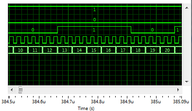
Run the VI with simulated I/O or create a testbench on the PC host to apply a test sequence as the FPGA VI input and monitor the resulting output sequence.

Simulate an FPGA VI
FPGA procedure

Debug your FPGA VI before compiling to a bitfile using execution highlighting, breakpoints, probes, and sampling probes.
The PC VI interacts with the FPGA VI in simulation mode to apply a test sequence as the FPGA VI input and monitor the resulting output sequence.

Compile an FPGA VI
FPGA procedure

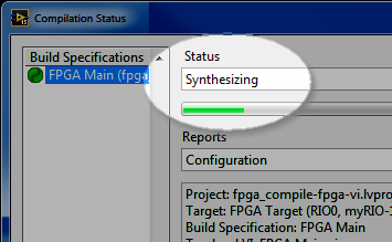
Compile your FPGA VI to a bitfile using your own computer or a cloud-based compiler.
Use a derived clock domain to effectively speed up or slow down the FPGA's 40-MHz clock for a selected portion of the FPGA block diagram.
Reuse (import) VHDL code and configure Xilinx IP blocks as drop-in components on the LabVIEW block diagram.
Reuse existing and validated VHDL-based circuit functionality in the FPGA block diagram instead of developing new LabVIEW G code to implement the same functionality.
Configure and use Xilinx IP (intellectual property) modules designed specifically for the Xilinx Zynq FPGA
Add your own functionality to the default Academic RIO Device FPGA "personality" (bitfile) to retain selected Device Express VI capabilities.
Use a local variable (front-panel indicator) to communicate between two parallel process loops contained within the same VI.
Use a global variable to communicate between two parallel process loops contained within different VIs under the same target.
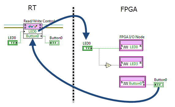
The RT VI operates (writes) the front-panel controls of the FPGA VI and reads its indicators.
Efficiently transfer blocks of data between the RT and FPGA by direct memory access (DMA) first-in first-out (FIFO) buffers.
Load and run a modified version of the default Academic RIO Device personality (FPGA bitfile) augmented by user-defined functionality, for example, to make a high-precision measurement of pulse width.
Transfer data, commands, and status between the FPGA target and a host system (RT or PC).
The PC VI operates (writes) the front-panel controls of the FPGA VI and reads its indicators.
Efficiently transfer blocks of data between the PC and FPGA by direct memory access (DMA) first-in first-out (FIFO) buffers.